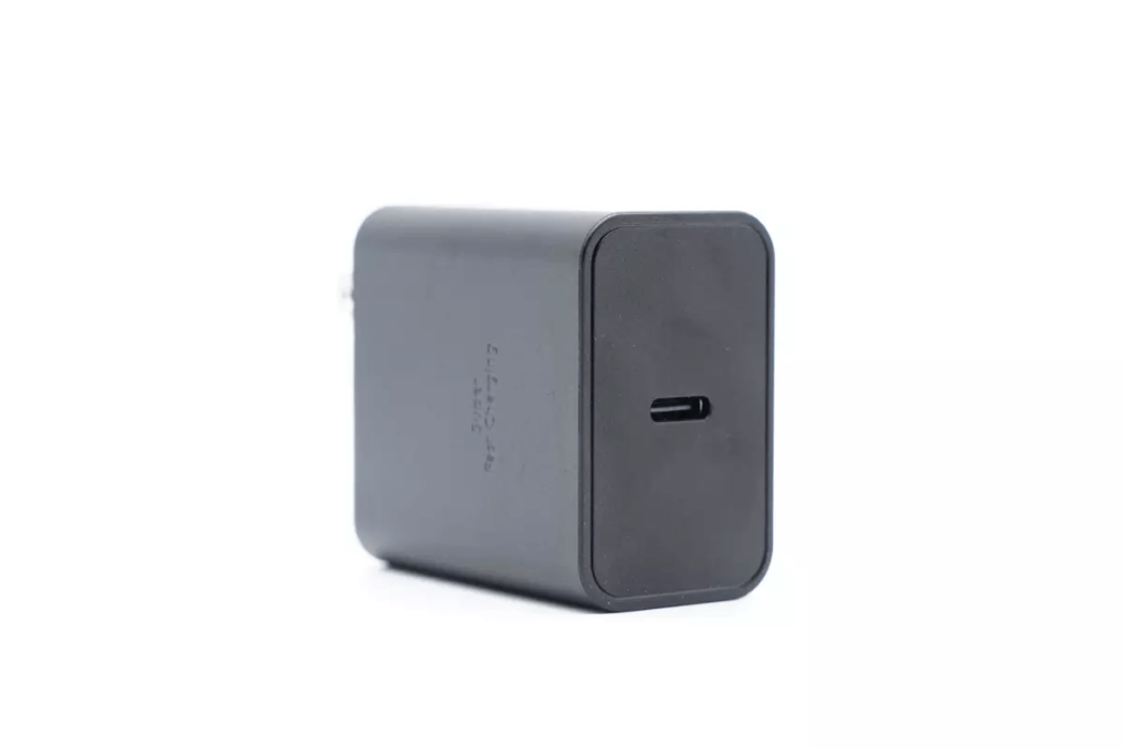
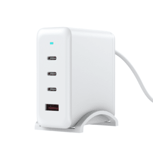
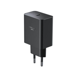
Wandkey 45W GaN charger features a black casing and a fixed plug design. The charger has a single output port and supports PD, PPS fast charging, Huawei FCP, Samsung AFC fast charging, and QC fast charging. With comprehensive support for various fast charging protocols, it can meet the charging needs of both smartphones and laptops. Below, we will teardown of a 45W GaN Charger to examine its internal design in detail.
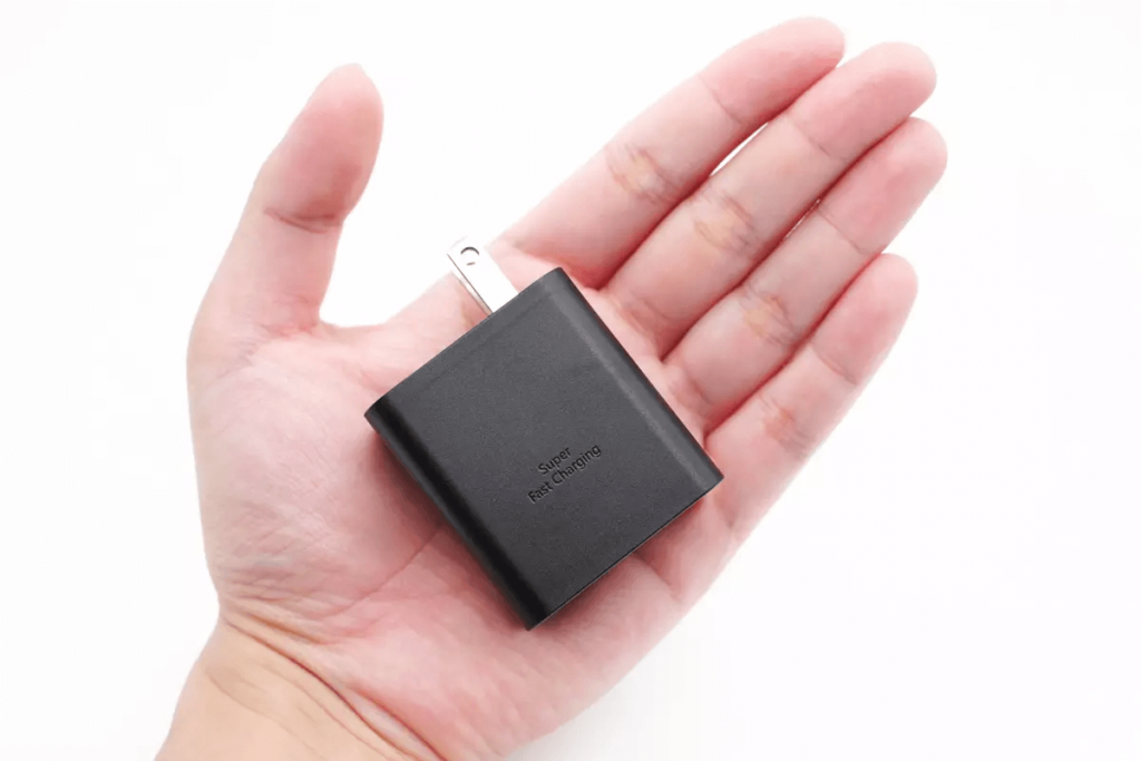
The 45w Gan charger uses a black shell made of PC flame-retardant material, and the entire black surface is matte-finished. With Super Fast Charging on the product.
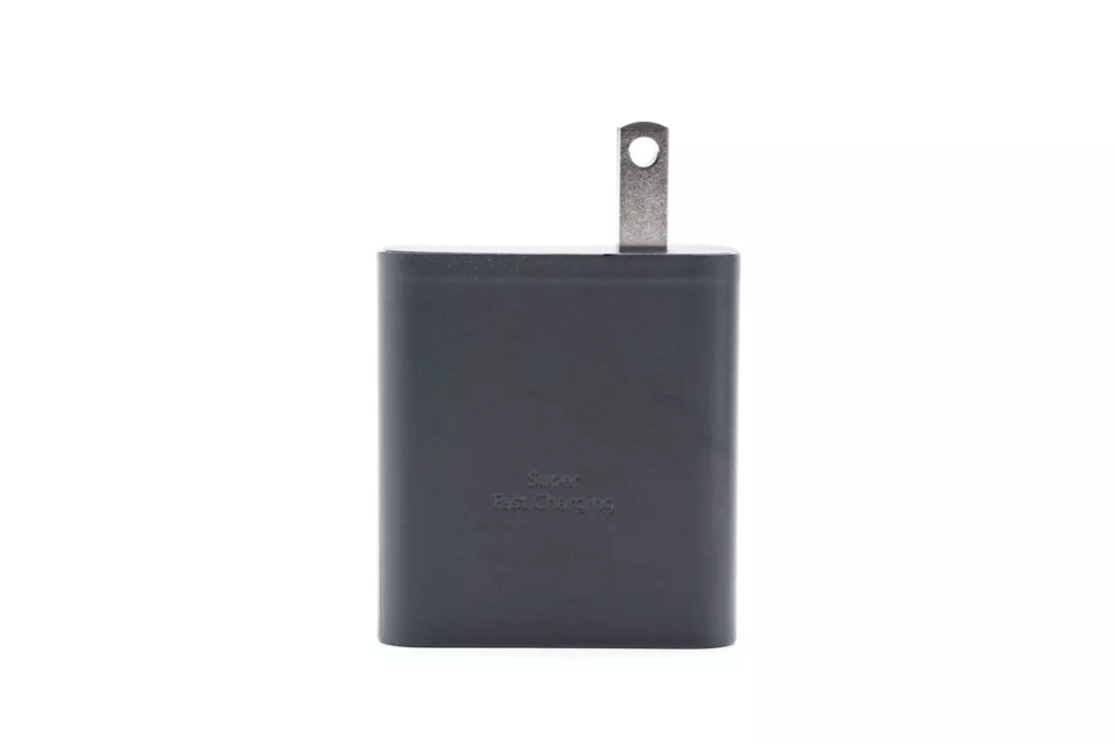
- Input: 100-240V~50/60Hz 1.2A
- Output: 5V3A, 9V3A, 15V3A, 20V2.25A
- PPS: 3.3-20V2.25A (7.5-45W)
- Total Output: 45W Max
- ETL/FCC/CE/ROHS certificate
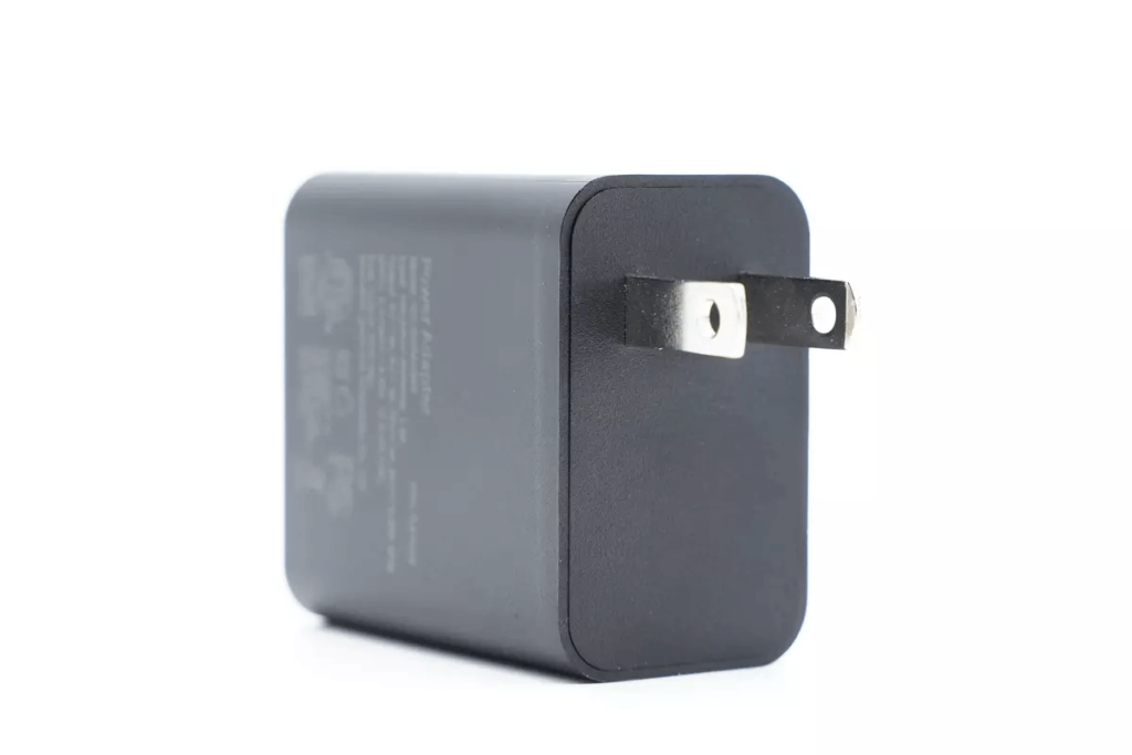
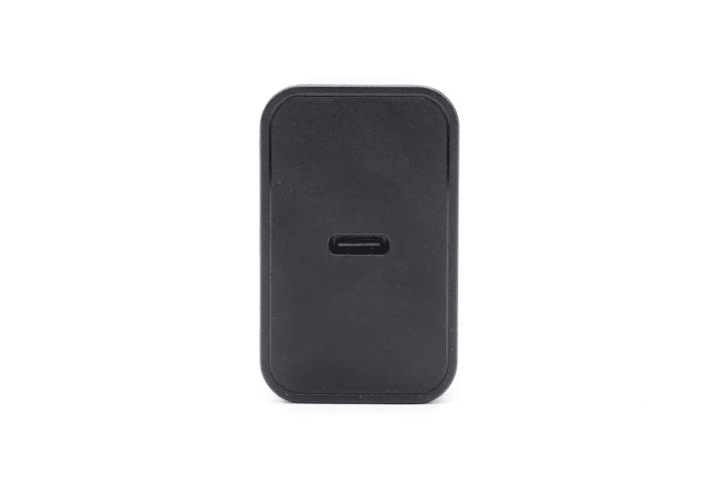
The size of 45w charger is 48.75*44.94*27.91mm

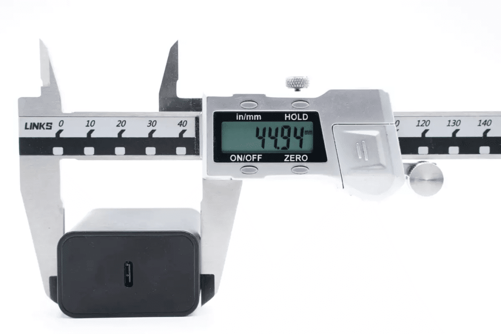
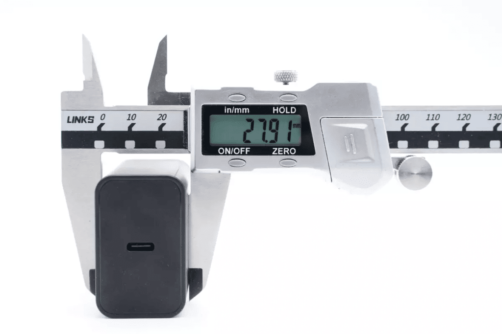
Compact Design: Lightweight and portable, perfect for travel and on-the-go use. The weight is 73G
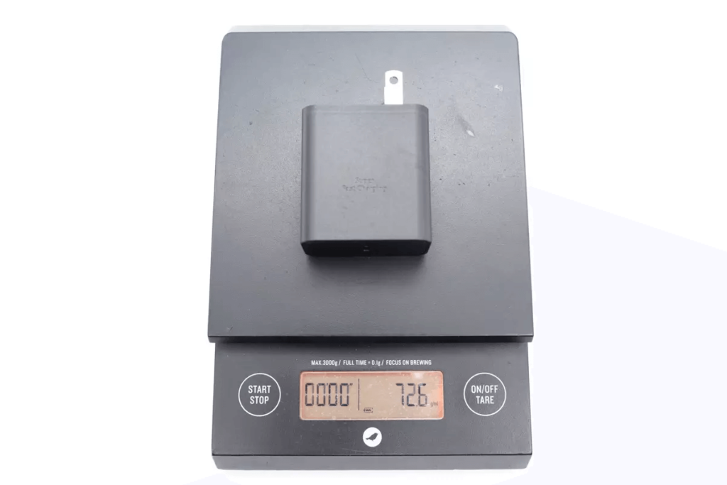
The 45W USB-C Charger supports FCP, AFC, QC3+, PD3.0, PPS, and QC4+ charging protocols.
It also has 4 fixed voltage levels: 5V3A, 9V3A, 15V3A, and 20V2.25A, as well as three PPS voltage levels: 3.3-11V5A, 3.3-16V3A, and 3.3-21V2.25A.
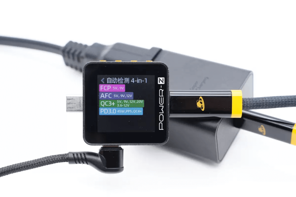
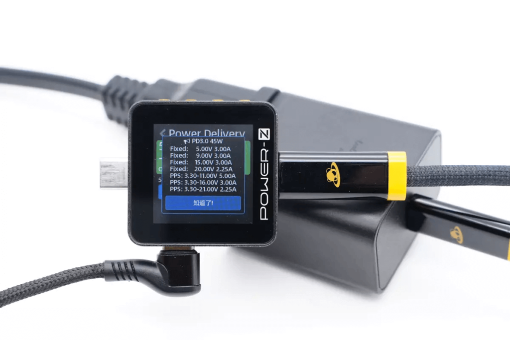
45W GaN charger teardown
After gaining a basic understanding of this 45W GaN charger, let’s proceed with the teardown to examine its internal design and materials
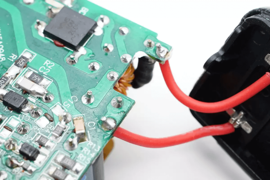
Open the shell along the seam on the side of the charger’s prongs. The prongs are connected to the PCBA module via soldered wires
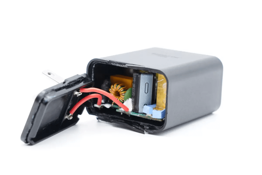
AC input wire solder joint close-up.
A brass heatsink is soldered and fixed above the PCBA module to dissipate heat for the transformer and GaN chip.

A thermal pad is placed between the heatsink and the transformer.
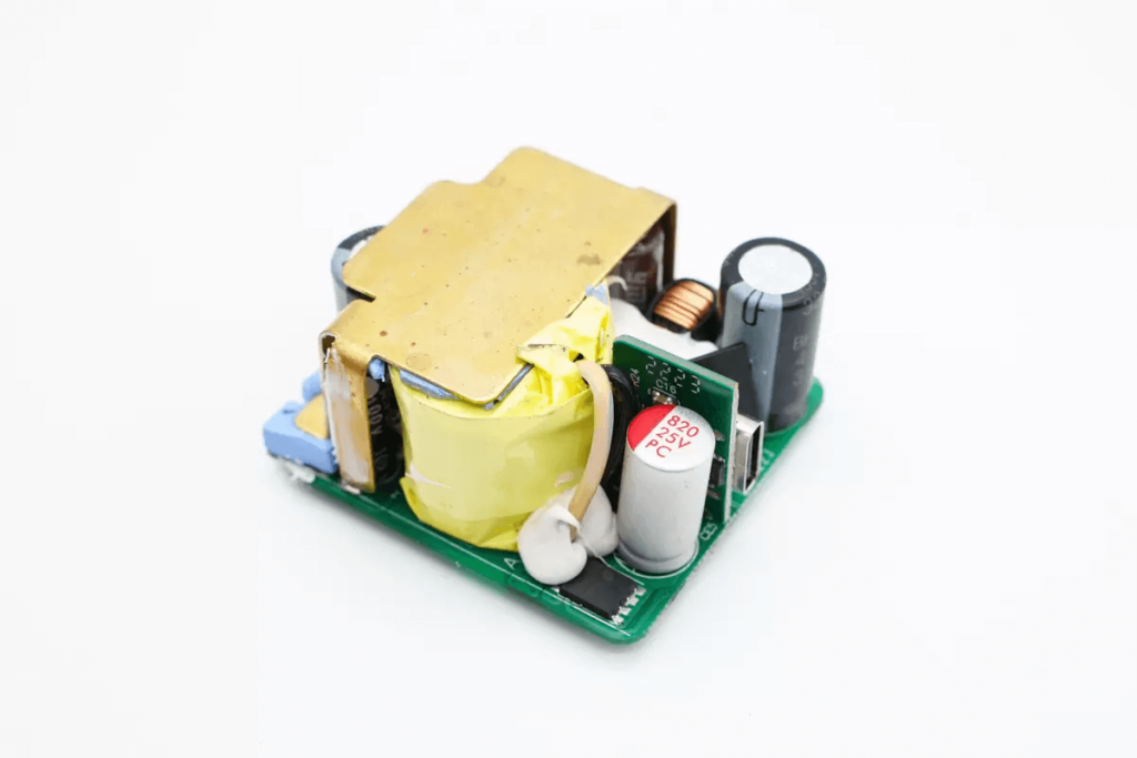
The brass heatsink is secured by soldering.
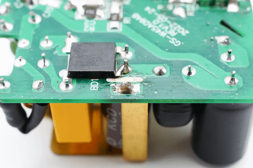
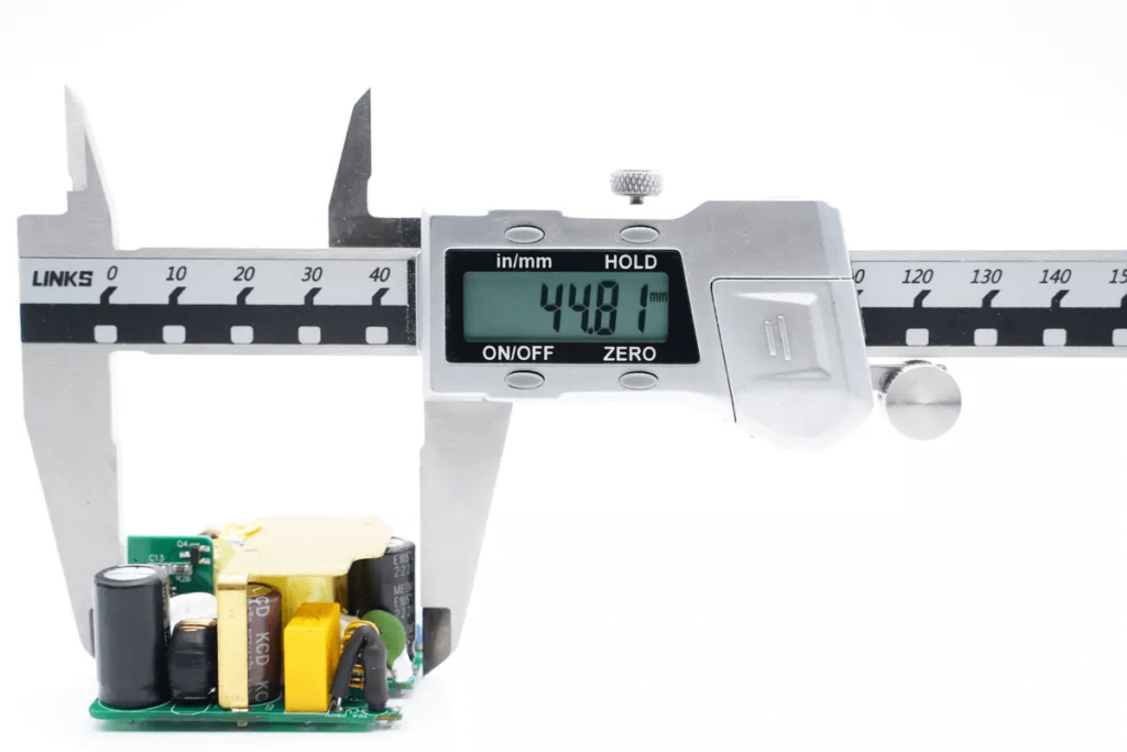
PCB size is 44.8*39.9*24.5mm
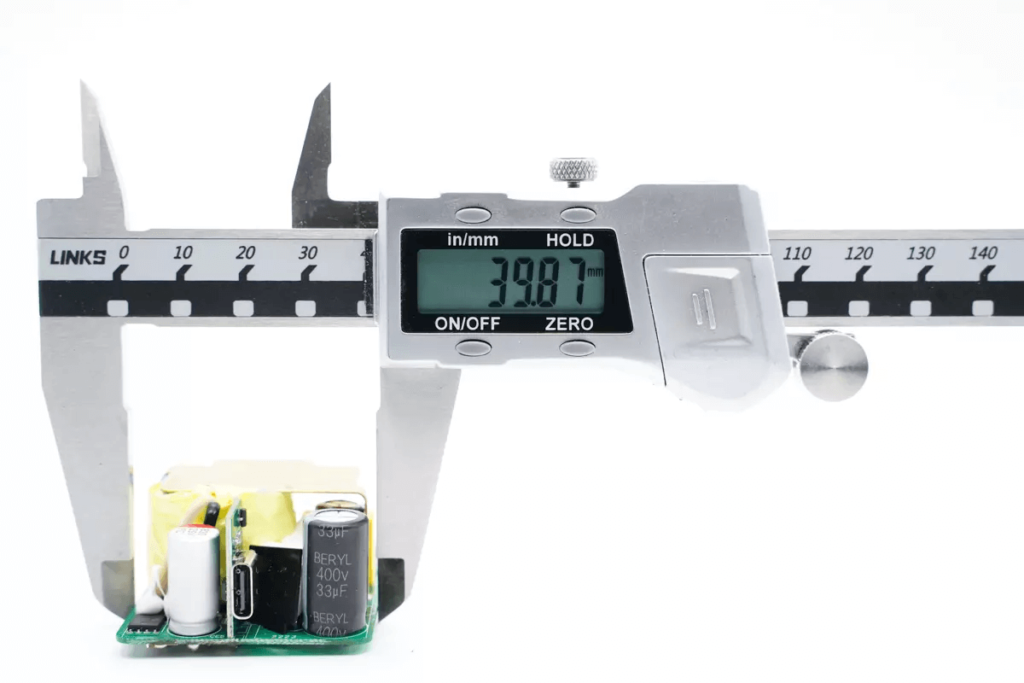
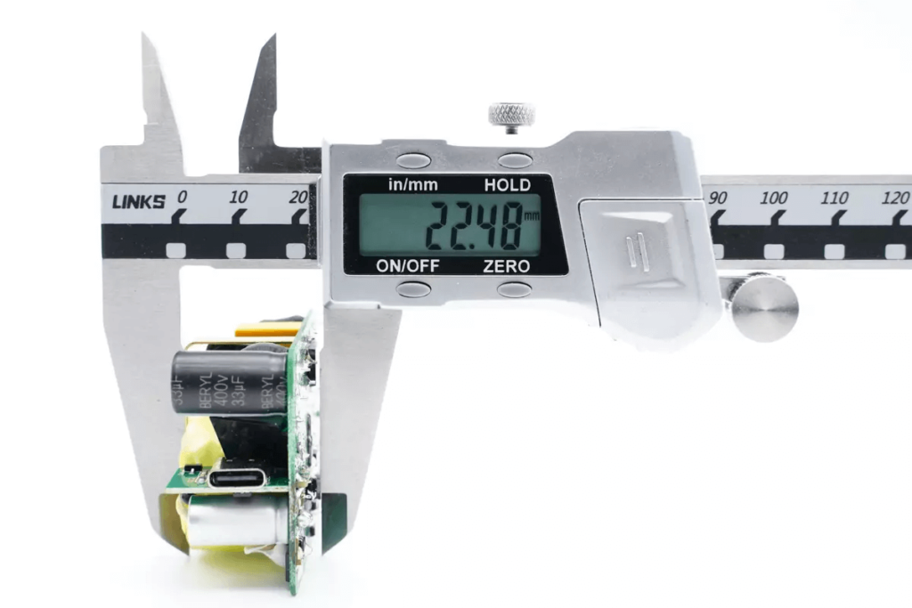
Remove the heatsink covering the transformer by desoldering it and continue with the teardown. The GaN chip, covered with a blue thermal pad, dissipates heat through the heatsink.
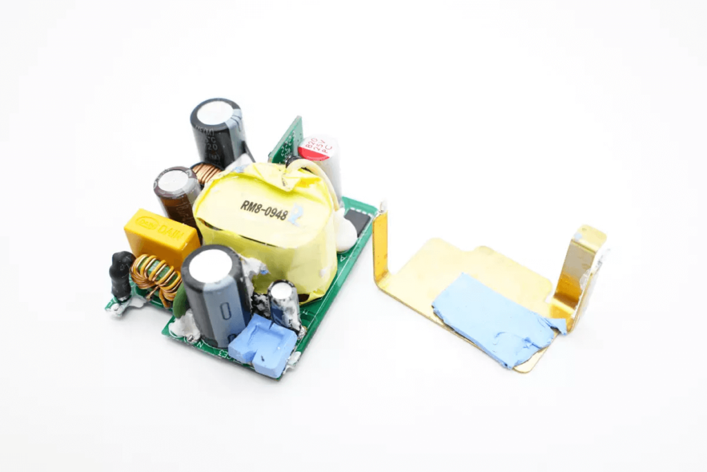
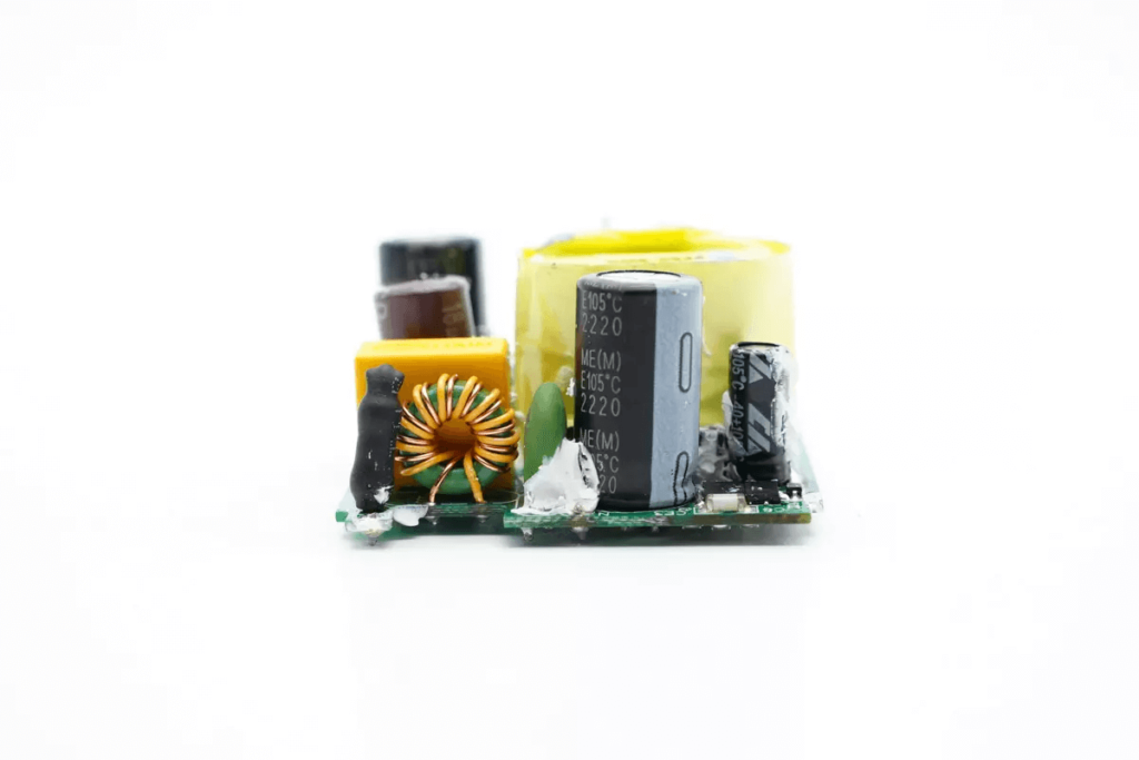
Front view of the PCBA module: the upper right corner has a soldered fuse, NTC thermistor, common mode inductor, and safety X2 capacitor. The left side contains the transformer, and below are the synchronous rectifier and output USB-C small board.
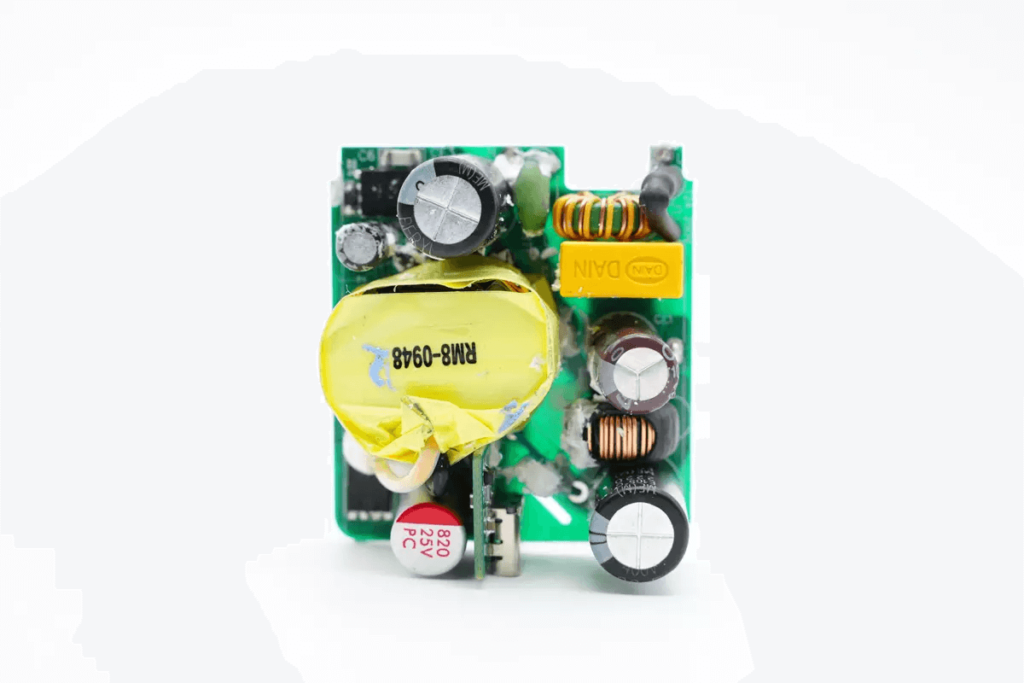
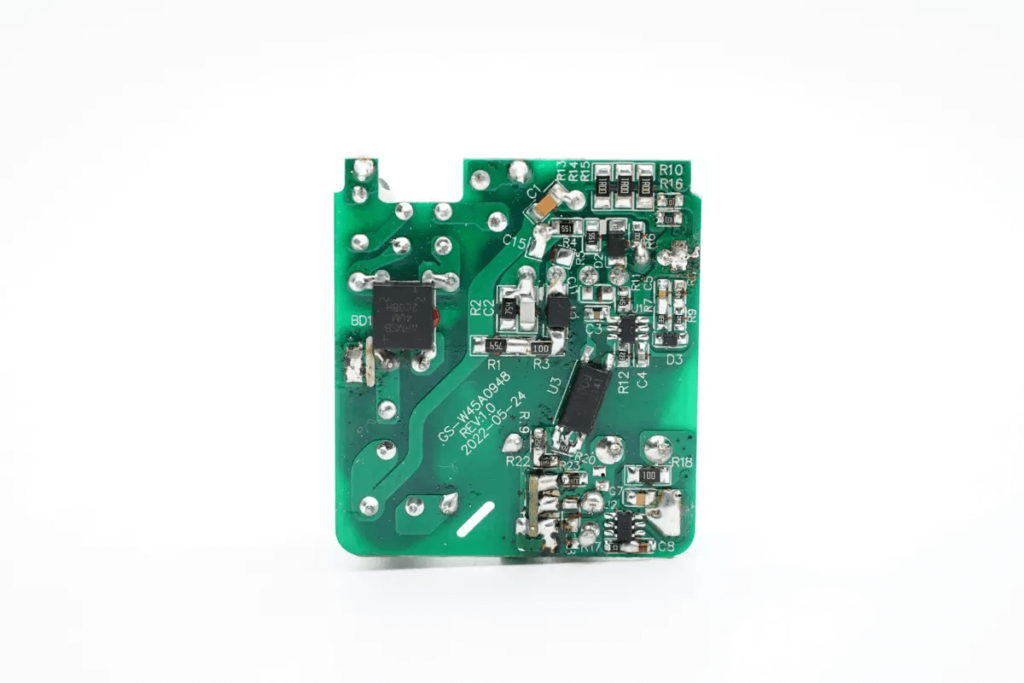
The back of the PCBA module has a soldered rectifier bridge, primary control chip, and feedback optocoupler. Observing the PCBA module, this 45W charger uses a high-frequency QR switching power supply and synchronous rectification architecture. The output voltage is regulated by the protocol chip through the optocoupler to meet the fast charging requirements at different voltages. Next, let’s start from the input end to understand the information of each component.
The input end of the charger has a soldered fuse, common mode inductor, and NTC thermistor, with a high-voltage filter capacitor soldered on the right side.
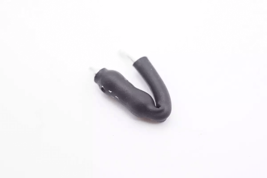
The input end has a time-delay fuse rated at 2A 250V, protected by heat shrink tubing.
The NTC thermistor is used to suppress the inrush current when the charger is powered on. It is from Zhiming, model 1R5D9, with a diameter of 9mm and a cold-state resistance of 1.5Ω.

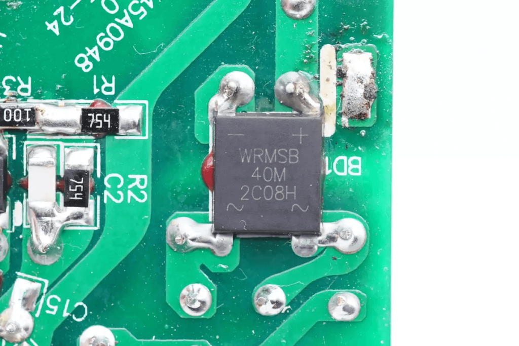
The rectifier bridge is soldered on the back of the PCB and is from Shenzhen World Industrial Co., Ltd., model WRMSB40M. This soft bridge, with its gentle recovery curve and smooth turn-off characteristics, can reduce the junction capacitance of the diode, resulting in minimal harmonic oscillation.
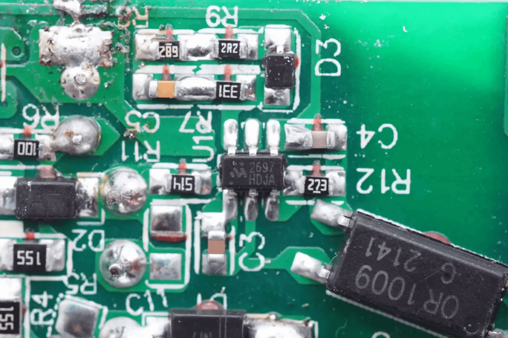
The primary control chip uses the MK2697G from Maorui Xin. It is a high-frequency QR AC-DC PWM control chip with an extremely small SOT23-6 package. It has a Vcc voltage tolerance of 110V and supports 9-90V Vcc power supply without the need for an external voltage regulator circuit, reducing board space and making it more flexible to use. It employs patented drive technology, supports direct drive enhanced GaN power devices, and optimizes SR Vds stress, effectively improving product efficiency and power density.
The MK2697G from Maorui Xin features adaptive multi-mode characteristics to meet the efficiency requirements of PD fast charging at different output voltages. Its 200KHz operating frequency fully leverages the advantages of GaN switching transistors, improving efficiency and reducing adapter size.
The MK2697G also includes protection functions such as output overvoltage, overpower, VCC overvoltage, input overvoltage protection, and synchronous rectifier short-circuit protection. It is suitable for USB PD chargers and high power density power applications.
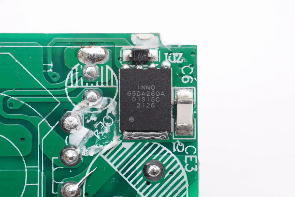
The GaN switch transistor uses the INN650DA260A from Innoscience. This is a cost-effective, 650V GaN high-voltage single transistor with a transient voltage tolerance of 750V. Thanks to process improvements, it has significantly better performance compared to previous GaN devices from Innoscience, making it suitable for 65-120W flyback and 120-200W LLC architectures.
The INN650DA260A supports ultra-high switching frequencies, has no reverse recovery charge, and features extremely low gate charge and output charge. It meets JEDEC standards for industrial applications, has built-in ESD protection, and complies with RoHS, lead-free, and EU REACH regulations.
The INN650DA260A from Innoscience uses a DFN56 package, which is significantly smaller than the DFN88 package, resulting in a substantial increase in power density. It can be used in switching power supplies, DC-DC conversion, totem-pole PFC, battery fast charging, and high-efficiency high-power density power conversion applications.
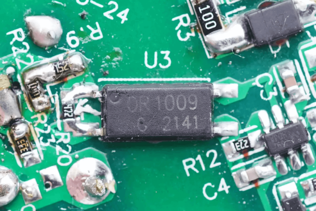
The OR1009 is used for output voltage feedback regulation.
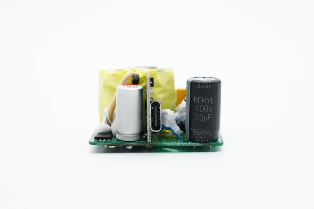
The output side has soldered solid-state filter capacitors and a USB-C female connector small board.
The back of the small board has a soldered protocol chip, current sensing resistors, and VBUS switch transistors.
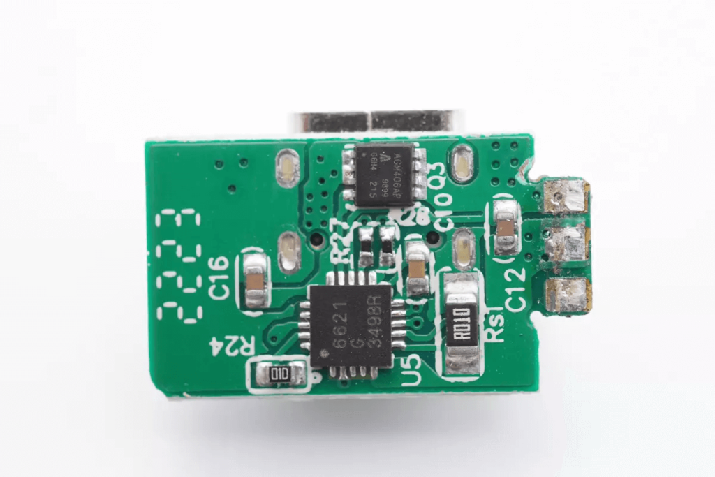
The protocol chip is from Tianyu, model JD6621. It is a highly integrated USB PD protocol chip that supports PD3.0 and PPS fast charging protocols, with TID: 3543. It supports an output voltage range of 3.3-21V. The JD6621 integrates Huawei SCP, FCP fast charging protocols, and Qualcomm QC2.0/3.0/QC5 fast charging, supporting fast charging applications from 20 to 100W.
The JD6621 has advantages such as multiple-time programming (MTP) and temperature detection (NTC) for power reduction. Additionally, it has two extra GPIOs for signal detection and ADC functions, meeting more customized product requirements.
The JD6621 supports output PDO selection, has multi-output port control functions, and integrates constant voltage and constant current control. The chip also includes overvoltage protection, undervoltage protection, overcurrent protection, short-circuit protection, and over-temperature protection. It uses a TQFN4*4-20L package and is suitable for USB PD fast charging, car chargers, and energy storage power applications.
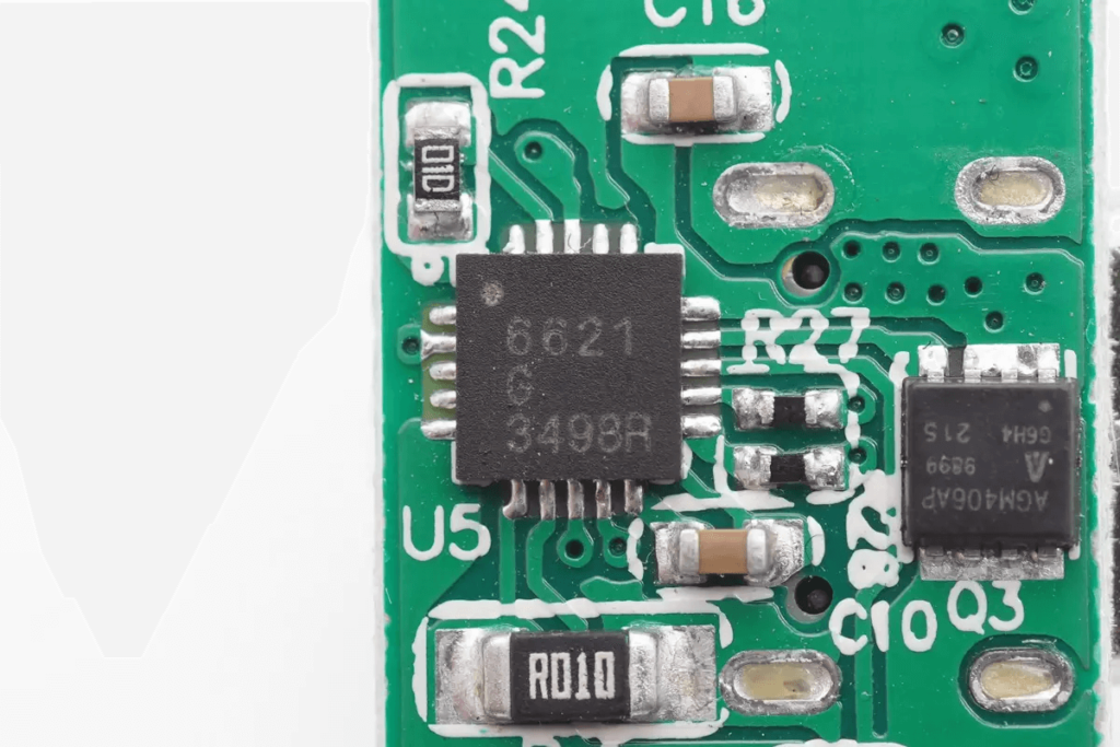
The VBUS switch transistor is from Chipown, model AGM406AP. It is a 40V NMOS transistor in a DFN3.3*3.3 package.

Conclusion
This 45W GaN charger features a fixed US plug design and a black shell with a simple design. The charger has a single USB-C port and supports FCP, AFC, QC3+, PD3.0, PPS, and QC4+ charging protocols. It also has four fixed voltage levels: 5V3A, 9V3A, 15V3A, and 20V2.25A, as well as three PPS voltage levels: 3.3-11V5A, 3.3-16V3A, and 3.3-21V2.25A, meeting the fast charging needs of Android phones and laptops.
Related Products
Wandkey Electronic Co.,Ltd is a specialized manufacturer of phone accessories, including MFI Certified iPhone Lightning Cables, USB Type-C Cables (2.0/3.0/3.1/3.2 Gen 2/USB4), Micro USB Cables, PD Fast Charging Gan Wall Chargers, Car Chargers, and more. Our products are UL/CE/RoHS/FCC/UKCA certified, ensuring the highest level of quality and safety. supports OEM/ODM service, printing logo, customized packaging, color, length, mould etc. Welcome to contact us get the quotation and samples for the test.
Any questions feel free to contact us, we would be happy to solve your issues
Top Topics
2024 Latest MFi Authorized Manufacturers list
Differences of Lightning Connector
How to check MFI Certification
How to get MFI Certification for Your Brand?
Why does the MFI Certified Lightning Cable so expensive?
MFI Product Packaging Requirement?
Disassemble MFI Lightning Cable
How do we guarantee the quality?
How to identify counterfeit or uncertified Lightning connector accessories
How to Choose Fast Charging Cable for Your Phone
How do I choose a USB-C cable?
Differences between USB 3.0 3.1 and 3.2
Test on USB C to USB C 3.1 Cable

